
Six Steps in Manufacturing a Thick Film Hybrid
» What is a Hybrid? » Thick Film Technology » Why choose Thick Film Technology? » Thick Film Technology
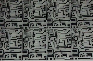
STEP 1: Schematic & Artwork
Similar to that done for Printed Circuit Boards PCB’s. The schematic diagram is drawn and then the artwork made up. The artwork is then transferred to a set of screens to enable the printing and firing process sequence to commence. Below is an example of artwork that has been prepared for a new hybrid.
STEP 2: Printing & Firing
The printing and firing of the hybrid ceramics is like that done for the pottery business. A print occurs, then firing in an oven, then second print, then firing in the oven, etc. This cycle depends on the complexity of the hybrid circuit. Printing and firing multiple layers consists of conductors, resistors, insulators and surface protection glasses.
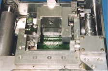
Automatic Printing
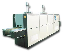
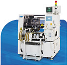
BTU Engineering specialty hybrid furnace
STEP 3: Laser Trimming
Setting the value and tolerance of resistors in the circuit by cutting a track in the fired resistor ink using a computer controlled laser beam. This can also be used for final circuit calibration and testing. A wide range of resistor values from milliohms to gigaohms along with ratings of up to tens of thousands of volts and fractional ratio tolerances can be achieved.
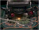
Laser Trimming
STEP 4: Surface mounting
Screen printing of solder paste, automated pick and place of surface mounted components on to the substrate and reflow soldering of the components.
JUKI Pick and Place machine
STEP 5: Pin attach
Adding lead frames (pins/legs) and soldering.
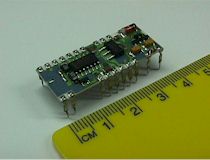
Hybrid with lead frames (pins/legs) attached
STEP 6: Manual Processing
Includes soldering of large components, washing, inspection, encapsulation, labelling, testing, burn-in, quality assurance, packing and shipping.
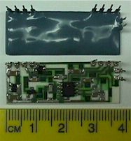
Hybrid Before & After Encapsulation
Additional Step in Manufacturing
Hybrids using semiconductor processes have the additional steps of semiconductor die attach, wire bonding and semiconductor encapsulation.
Hybrid Electronics Australia Pty. Ltd. Factory 6, 56 Smith
Road, Springvale Victoria 3171 Australia
Ph: +61 (3) 9574 2232 E-mail: hybrid@hybrid-electronics.com
© Copyright 2017 Hybrid Electronics Australia Pty Ltd. All rights reserved.
The content and format of this website are subject to copyright and may not be reproduced without permission.
Site designed and developed by Cast Creative Multimedia Solutions Pty Ltd